
Fermi Level Pinning
The vacancies are only created by the high-temperature anneal. Fermi Level Pinning expresses the fact that the metal workfunction changes in magnitude when you replace SiO2 by HfSiO4 in a metalSiO2SC-stack irrespective of the metal itself materialetc.

Pin On Constellations
The Fermi-level pinning for electronegative pFET metals is now thought to be an extrinsic effect due to oxygen vacancies and band-bending in the oxide Akasaka et al 2006.
Fermi level pinning. Fermi-level pinning in high-work-function materials is governed by the O vacancy generation and subsequent formation of interface dipoles near gate electrodes due to the electron transfer. We also quantitatively compared our results with the theoretical simulation results of the monolayer structure. In conventional contacts to bulk metals the 2D semiconductor Fermi levels become pinned inside the bandgap deviating from the ideal SchottkyMott rule and resulting in significant suppression of carrier transport in the device.
The pinning positions for 110 GaAs are 075eV and 055eV above the valence band for n-and p-type materials respectively 15. The reason is that Φ is generally determined by the energy difference between the Fermi level FL and the semiconductor band edges in the junction 1 where Φ e and Φ h are the barrier heights for. This problem disturbs the basic MOSFET-operation because of several reasons.
On the other hand O interstitial formation plays a crucial role for Fermi-level pinning in low-work-function materials. Robertson et al 2007. The SE yield characterisation revealed two major features.
Shiraishi et al 2004. Here we report the experimental study on Fermi level pinning of monolayer MoS 2 and MoTe 2 by interpreting the thermionic emission results. This is called Fermi level pinning at the M-S interface.
The impacts of the charge transfer mechanism on Fermi-level pinning were confirmed for the gas molecules adsorbed on monolayer WS2. High Speed Devices and Circuits. Until now Fermi level pinning of monolayer TMDCs has been reported only theoretically although that of bulk TMDCs has been reported experimentally.
It has been shown that a high number of Pb 0 at the surface leads to Fermi-level pinning 1835 and n-type doping. It doesnt matter how lightly or how heavily doped your semiconductor your Fermi level will always get stuck at that energy level. Despite the bonding in TMDCs being largely constrained within the layers strong Fermi-level pinning FLP was observed in TMDC-based devices reducing the tunability of the Schottky barrier height.
The proposed mechanism governing Fermi-level pinning is applicable to the systems of adsorbates on recently developed two-dimensional materials such as graphene and transition metal dichalcogenides. How strongly the barrier height B depends on the metal. Shiraishi et al 2004The vacancies are only created by the high-temperature anneal.
For the 110 InAs sur-face the Fermi level is fixed at 013eV above the bottom of the conduction band for n-and p-type materials 16. Results indicate that pinning occurs due to the interfacial Si-Hf and. On one hand Fermi level pinning by a high density of extrinsic surface states on the H-terminated surface and on the other a.
The experiments reveal a very strong Fermi level pinning and the corresponding pinning factor is about 01 Nature 2018 557. This high number of Pb 0 surface states has only been observed with XPS on samples that were illuminated with light in UHV for a prolonged time. We present evidence that metal-induced gap states MIGS are the origin for the large FLP similar to conventional semiconductors.
For Al xGa 1xAs ternary alloys the Fermi level pinning has been. We report here that Fermi pinning at the polysiliconmetal oxide interface causes high threshold voltages in MOSFET devices. In a nutshell Fermi-level pinning refers to the equilibrium condition of the free surface of a semiconductor which is different from the equilibrium condition in the bulk.
Fermi level aligning with a characteristic energy position Eo of the semiconductor exists making the value of SBH inde-pendent of or weakly dependent on the metal work function. The Fermi-level pinning for electronegative pFET metals is now thought to be an extrinsic effect due to oxygen vacancies and band-bending in the oxide Akasaka et al 2006. The free surface or interface of a semiconductor does not have a band gap between conduction and valence bands to see why read the extended explanation below.
That phenomenon is called the Fermi level pinning and it takes away a very very important degree of freedom for engineering for semiconductor devices. 696700 but all the existing calculations give a larger pinning. Robertson et al 2007.

Ergolding Secondary School By Behnisch Architekten And Leinhaupl Neuber High School Design Secondary School School Plan

Music History Of Philosophy And Google Search On Pinterest

Til That The Definition Of 1 Second Is 9 192 631 770 Oscillations Of The Standard Cesium 133 Atom The Basis F Reflection And Refraction Time Travel Flip Book

Pin On Leibal Featuring Minimal And Functional Designs

Dark Matter Dark Matter Astrophysics Physics Theories

What Are The Healthiest Sleeping Positions Infographic Healthy Sleeping Positions Ways To Sleep Sleeping Positions

Http Media Rightmove Co Uk 58k 57154 28179236 57154 260823 Flp 00 0003 Png Maine House Charlwood How To Plan

Lena Kohl Christiane Muller Hannah Rochelt Louisen School Munich Main Station 2016 This Proj School Floor Plan School Building Plans School Building Design

Theberry Healthy Sleeping Positions Ways To Sleep Sleeping Positions

The Drake Equation Poster On Behance Drake Equation Physics Facts Physics Topics

Al Ni Phase Diagram God S Gift To The Metallurgist Diagram Chart Science

What Is Taqwa Beliefs Ramadan Islam Muslim

12 Strangely Beautiful Alien Worlds You Really Wouldn T Want To Live On Dark Planet Planets Alien Planet

Bridal Hairstyle For Round Face Latest Hairstyles And Haircuts For Pakistani Bridal Makeup Wedding Makeup Blue Wedding Makeup Bridesmaid

I Can T Help Feeling That Other Life Is So Close Saturn Astronomy Saturns Moons

Night Club Wintergarden Istanbul Turkey A Cakir Likely Unbuilt N D Stratton O Hammon Photograph Co Architecture Collection Parking Design Architecture
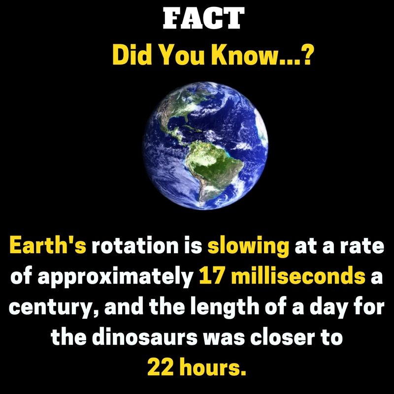
Fact Earth S Rotation Is Slowing At A Rate Of Approximately 17 Milliseconds A Century And The Length Of A Day For The Din Earths Rotation Facts Space Facts

One More Sunrise Taken November 9 2013 My Last Full Day On Iss Kn From Space Earth From Space Cool Pictures Life In Space

Pin On Science
Post a Comment